반도체/FPGA - Verilog
[FPGA] 시프트 레지스터 Shift Register - SIPO/PISO
쑨야미
2021. 3. 11. 12:58
통신에 많이 이용되는 Shift Register를 Verilog를 이용하여 FPGA 설계를 해보겠습니다. [Schematic - Simulation - Code]
Shift Register
시프트 레지스터는 직렬과 병렬 인터페이스를 전환하는 데 가장 일반적으로 사용된다. 이것은 많은 회로가 병렬 비트의 집합으로 동작하기 때문에 유용하지만, 직렬 인터페이스의 구성이 더 간단하다. 시프트 레지스터는 간단한 지연 회로처럼 사용될 수 있다. 몇몇 양방향 시프트 레지스터는 스택의 하드웨어 구현을 위해서 병렬로 연결할 수도 있다.
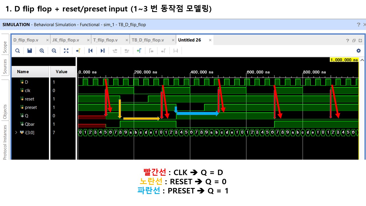
D FLIP FLOP
- clock의 Positive Edge 지점에서 D(data)의 Level(High or Low)를 출력
사용예시 -> uart 통신 (74hc595)

SIPO = Serial Input Parallel Output
PISO = Parallel Input Serial Output
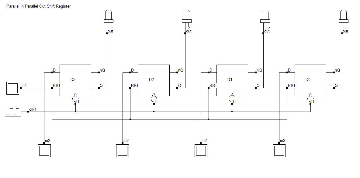
SIPO
- SIPO Schmatic
- SIPO simulation

Enable High 구간에서 clk 가 Rising Edge 일때마다 비트이동 후 4개의 병렬 output 생성(5부근)
- code
module shift_register_SIPO(
    input D,
    input clk,
    input E,
    input reset,
    //input preset,
    output [3:0] Q
    //inout [3:0]Q
    );

    wire clk_in;
    reg preset;

    and(clk_in, clk, E);
    D_flip_flop D3 (.D(D), .clk(clk_in), .reset(reset), .preset(preset), .Q(Q[3]));
    D_flip_flop D2 (.D(Q[3]), .clk(clk_in), .reset(reset), .preset(preset), .Q(Q[2]));
    D_flip_flop D1 (.D(Q[2]), .clk(clk_in), .reset(reset), .preset(preset), .Q(Q[1]));
    D_flip_flop D0 (.D(Q[1]), .clk(clk_in), .reset(reset), .preset(preset), .Q(Q[0]));

    initial preset = 1 ;

endmodule
PISO
1) Preset 과 Enable 로 구현된 PISO
- PISO 1) Schmatic

- 정확히 이 회로도를 구현하자면, Enable 핀은 clk핀과 AND로 묶이고, Enable에 Not 게이트를 하여 핀을 뽑아, 입력단자들과 nand로 묶어 Preset에 넣어줘야한다.
- Enable이 High level 일때, clk에 의해 비트가 이동되며
- Enable이 Low level 일때, preset단자에는 Data가 입력이된다.
- preset이 1이면 이전 Data가 Q에 입력이되고/ 0이면 Q에 1이 입력이 된다.
- PISO 1) Simulation

- PISO 1) code
module shift_register_PISO(
    input [3:0] D,
    input clk,
    input E,
    output Q
    );

    wire Ebar, clk_in, Q3, Q2, Q1;
    wire [3:0]in;

    //reg reset;

    not (Ebar, E);
    and (clk_in, clk, E);
    nand (in[0], Ebar, D[0]);
    nand (in[1], Ebar, D[1]);
    nand (in[2], Ebar, D[2]);
    nand (in[3], Ebar, D[3]);
    D_flip_flop G3 (.D(1'b0), .clk(clk_in), .reset(1'b1), .preset(in[3]), .Q(Q3));
    D_flip_flop G2 (.D(Q3), .clk(clk_in), .reset(1'b1), .preset(in[2]), .Q(Q2));
    D_flip_flop G1 (.D(Q2), .clk(clk_in), .reset(1'b1), .preset(in[1]), .Q(Q1));
    D_flip_flop G0 (.D(Q1), .clk(clk_in), .reset(1'b1), .preset(in[0]), .Q(Q));

    //initial reset =1;

endmodule
2) Shift/Load로 구현된 PISO
- PISO 2) schematic

- PISO 2) simulation

- preset단자를 쓰지 않으면서 구현한 PISO Register이다.
- wirte일때(= ~shift )는 D0값을 계속 출력하고 있으며 , shift가 High 가되면 D1,D2,D3값이 출력이 된다. 그리고 shift가 low가 될때까지 D3값을 계속 출력한다.
- PISO 2) code
module shift_register_PISO_with_load(
    input [3:0] D,
    input clk,
    input shift,
    output Q
    );

    wire load, Q3, Q2, Q1;
    wire [2:0]in;
    wire [2:0]Din;
    wire [2:0]Qin;


    //reg reset;

    not (load, shift);

    and (Qin[2], shift, Q3);
    and (Qin[1], shift, Q2);
    and (Qin[0], shift, Q1);

    and (Din[2], load, D[2]);
    and (Din[1], load, D[1]);
    and (Din[0], load, D[0]);

    or  (in[2], Qin[2], Din[2]);
    or  (in[1], Qin[1], Din[1]);
    or  (in[0], Qin[0], Din[0]);

    D_flip_flop G3 (.D(D[3]), .clk(clk), .reset(1'b1), .preset(1'b1), .Q(Q3));
    D_flip_flop G2 (.D(in[2]), .clk(clk), .reset(1'b1), .preset(1'b1), .Q(Q2));
    D_flip_flop G1 (.D(in[1]), .clk(clk), .reset(1'b1), .preset(1'b1), .Q(Q1));
    D_flip_flop G0 (.D(in[0]), .clk(clk), .reset(1'b1), .preset(1'b1), .Q(Q));

    //initial reset =1;

endmodule